Q2
( a )
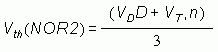
For a CMOS NOR2 gate, prove that if kn=kp and VT,n=|VT,p| then
5
( b )
Implement F = (A.B + C.D)' in CMOS.
WELCOME TO IP UNIVERSITY QUESTION PAPERS WEBSITE
Homepage : https://ippapers.tripod.com/ |
Back to VI semester papers
|
(Please write your Roll No. immediately) |
Roll No. .................................. |
Sixth Semester [B.Tech] - April 2006
|
Paper Code : ETEC – 310 Subject : VLSI Design |
|
Time : 11/2 Hours |
Maximum Marks : 30 |
|
Note : Attempt any 3 questions in all. Q1 is compulsory. Each question carries 10 marks. |
|
Q1 |
( a ) |
Compare the features of NMOS depletion-load logic gates and CMOS logic-gates. |
2 |
|
( b ) |
Compare the features of TG and NMOS pass devices. | 2 | |
| ( c ) | Discuss the parasitic capacitances SR-CMOS and the trise | 2 | |
| ( d ) | Charge storage and charge leakage with respect to NMOS pass transistors. | 2 | |
| ( e ) | Discuss DRAM operation modes. | 2 |
|
Q2 |
( a ) |
For a CMOS NOR2 gate, prove that if kn=kp and VT,n=|VT,p| then |
5 |
|
( b ) |
Implement F = (A.B + C.D)' in CMOS. |
5 |
|
Q3 |
( a ) |
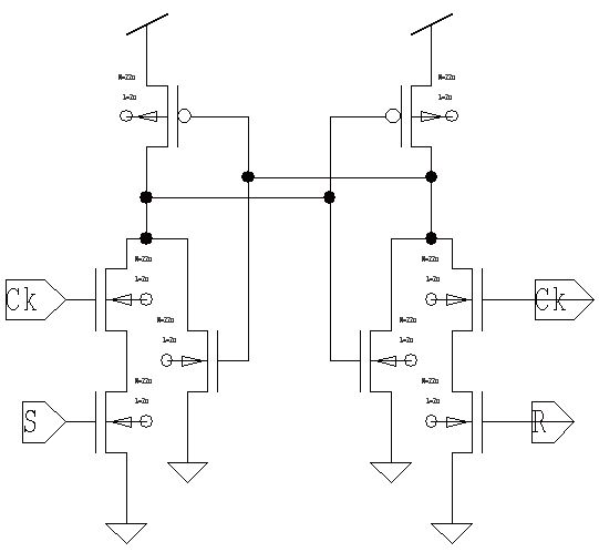
For the CMOS SR flip-flop, shown in figure 3, the four transistors
M5, M6, M7 and M8 have equal W/L ratios. Determine the minimum value
required for this ratio to ensure that the flip-flop will switch.
The other relevant parameters areas follows: u,=2.5 upCOX=50uA/V2 VT,n=|VT,p|=1V For M1 and M2 (W/L)n = 4u / 2u and for M3 and M4 (W/L)p = 10u / 2u
|
10 |
|
Q5 |
Write short notes on any two: |
10 |
|
|
( a ) |
Precharge and evaluate switch of Dynamic logic. |
|
|
|
( b ) |
Explain with a neat diagram the clocked D-latch employing TG and CMOS. |
|
|
|
( c ) |
With a neat timing diagram describe the operation of a 3-transistor DRAM cell. |
|